Terabit Embedded Nonvolatile Memory
Memory is one of the most fundamental solid-state devices and a key technology driver for the semiconductor industry.We are a world-renowned memory device research group with more than 15 years of research experience.
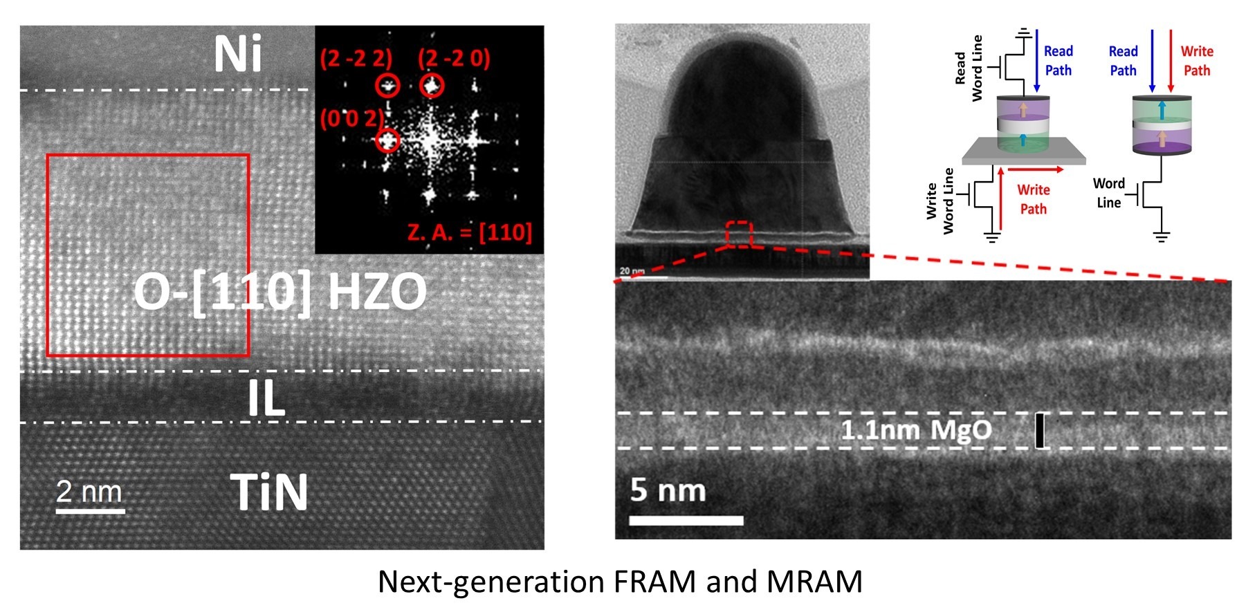
We are now focusing on the development of embedded memory technology that can be integrated into advanced logic nodes (<28 nm) with high density (>1 Tb), in particular Ferroelectric RAM (FRAM), Magnetoresistive RAM (MRAM), Resistive-switching RAM (RRAM) with low power consumption (
[1] Ultrahigh-density V-RRAM for storage-class memory [IEDM 2013]
[2] Modeling framework of ferroelectric tunnel junction (FTJ) [IEDM 2019]
[3] BEOL-compatible FeFET: MFMFET [IEDM 2020]
Artificial Intelligence and In-Memory Computing Chips
Today’s computer architecture is too outdated to support the workload of exascale or even future zetta-scale computing, general AI that has the cognitive capabilities like human beings, and distributed AIoTs with an extremely tight energy budget.
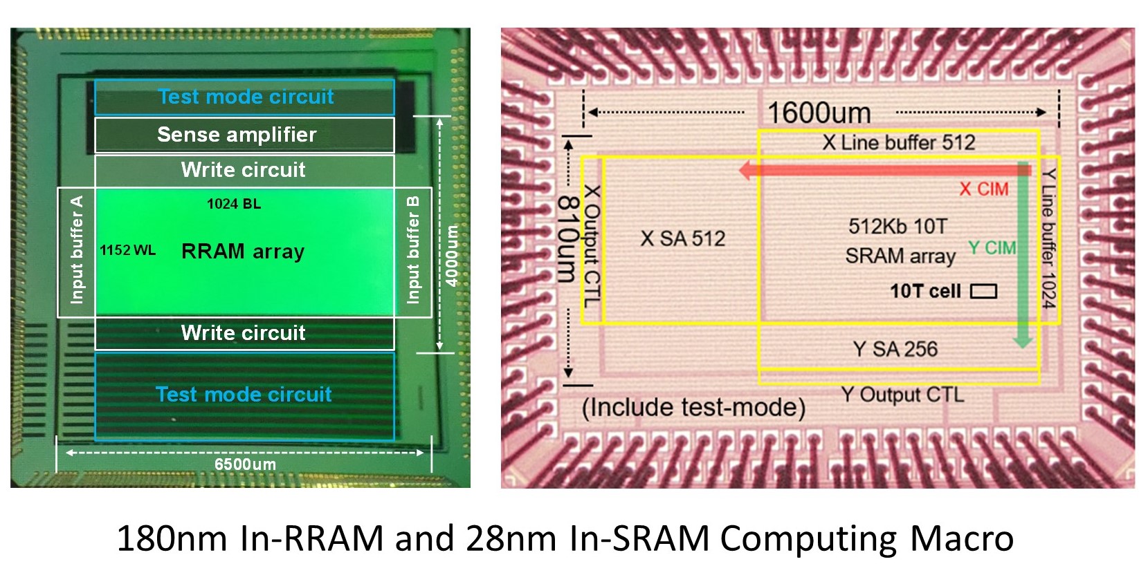
“Computer” literally means “Electrical Brain” in Chinese. We took the inspiration once again from the human brain and are developing a neuromorphic computing architecture called in-memory computing (IMC). IMC brings computing into memory in a way similar to our biological neural networks. By saving the latency and energy consumption associated with data movement and leveraging the efficient analog computing in memory arrays, IMC potential could be a thousand times more energy-efficient than today’s computers.
We are one of the very few selected groups in the world capable of performing cross-layer optimization for IMC designs. We have contributed several breakthroughs at device, circuit, algorithm, and application levels in this exciting field.
Two-dimensional Layered Materials and Devices
Since the discovery of Graphene in 2004, another new category of materials appeared on the horizon for designing advanced electronic devices: two-dimensional layered materials (2DMs). Examples are molybdenum disulfide (MoS2), tungsten diselenide (WSe2), etc. Because of their low-dimensional properties, these materials possess many unprecedented physical, electrical, optical, optoelectronic, and mechanical properties.
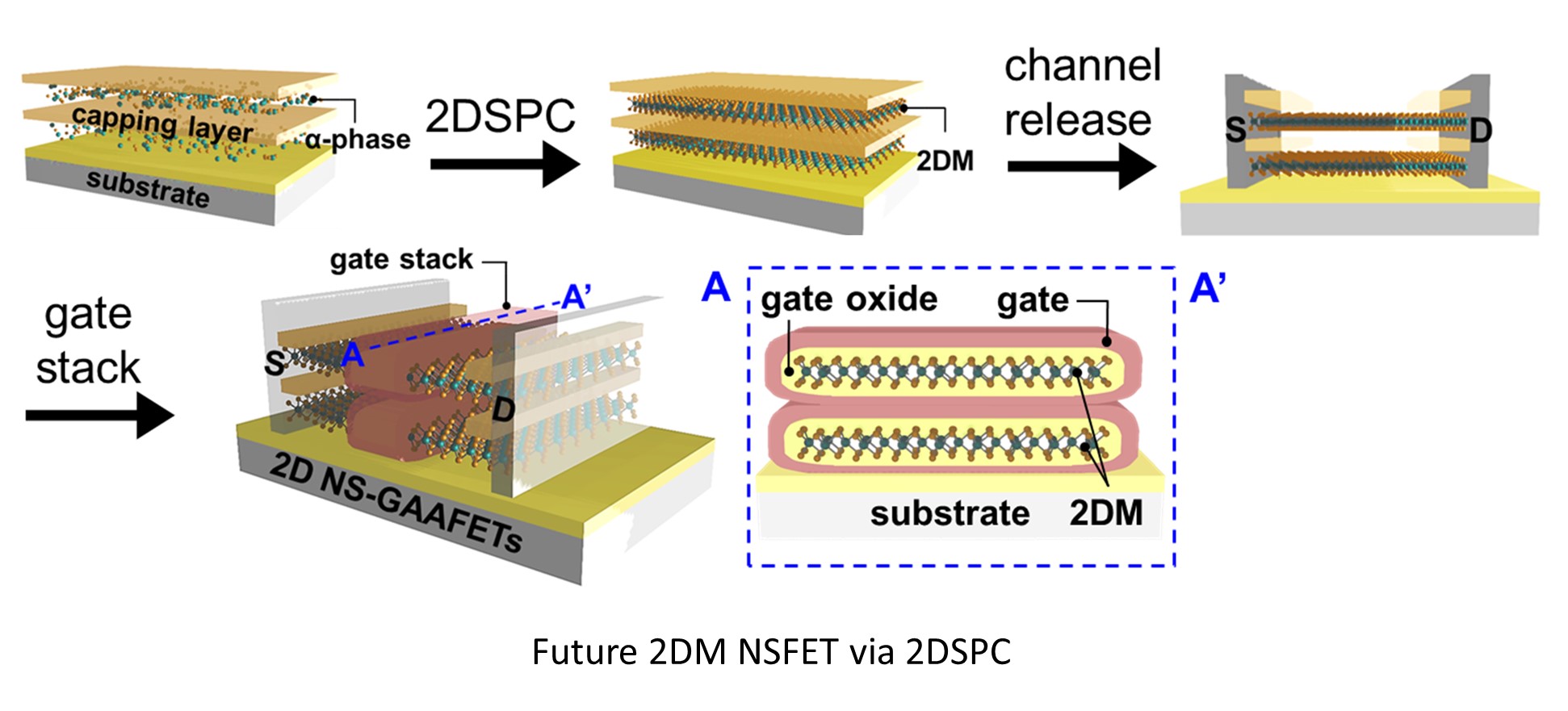
We are investigating the application of novel 2DMs as the channel materials in ultimately scaled transistors beyond the scaling path of three-dimensional crystalline silicon and also in new functional devices leveraging the unique properties in 2DMs.
Our group published the 1st 2DM device paper from Taiwan in IEDM 2014. We also pioneered a simple yet general synthesis route for large-scale and high-quality 2DMs, called 2DSPC. We believe 2DMs offer new exciting opportunities to continually push the limit of Moore’s law even farther.
BEOL-compatible Monolithic 3DIC
As the conventional two-dimensional scaling is approaching its limits in both physics and process feasibility, people are looking into the third dimension. Monolithic 3D (M3D) integration stacks devices vertically using only wafer-level processing technology. This approach offers the ultimate integration density among different 3D integration schemes.
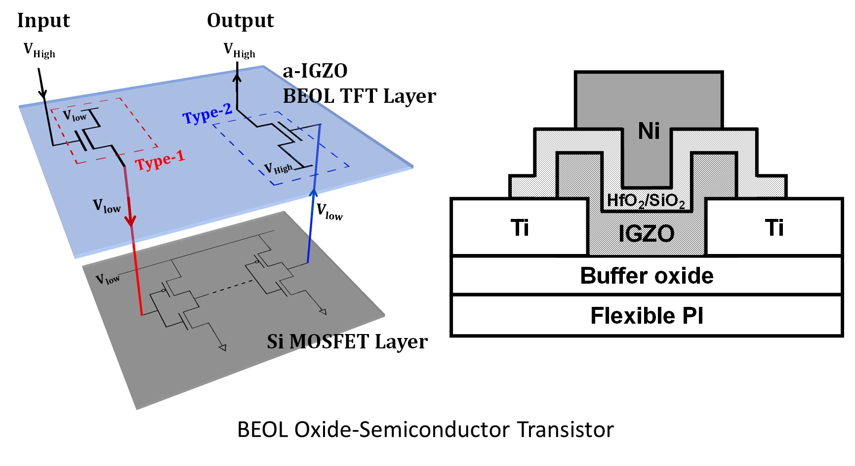
At this dawn of the M3D IC era, more and more functional devices have been integrated into back-end-of-line (BEOL) processes, which conventionally include only passive interconnects. The low-temperature oxide semiconductor (LTOS), such as indium-gallium-zinc oxide and indium oxide, is particularly suitable for BEOL-compatible M3D because of its low thermal budget in processes.
We have developed LTOS low-voltage logic gates, high-voltage transistors, memories, chemical sensors, and phototransistors. This versatile device toolbox in BEOL enriches the development of future M3D ICs.


